Posts

Showing posts from March, 2012

What is Instruction cycle

Image
Instruction cycle is the basic operating of computer who contain two cycle which are Fetch Cycle and Execute cycle . Fetch Cycle Fetch cycle is the cycle that fetch data or next instruction from the main memory into the CPU. During the Fetch Cycle ,there are 4 register are involved which are PC , MAR , MBR and IR . Generally the process in the Fetch Cycle can be depicted by: MAR ← PC (specify address in MM for the next read/write) MBR ← M (MAR) (data to be written/received from memory) PC ← PC + 1 (hold address to be fetched next. CPU increment the PC after each instruction) IR ← (MBR) (fetched instruction is loaded into register) Execute Cycle Execute cycle is the cycle that interpret the opcode and perform the indicated operation. The followings are steps that are involve in execute cycle: 1. Instruction decoding (to determine the operation that has to be performed by the CPU) 2. Operand (data) fetching 3. Data Processing 4. Store Resul

Bullet keyboard Shortcut key in Microsoft word

Image
There are many shortcut key you can use in Microsoft Word like Bullet shortcut key in Microsoft word (ctrl+shit+L). You also can customize your own shortcut key in Microsoft Word using the method below! To add bullet                : ctrl +Shift+L To remove the bullet  : ctrl +Shift+N You also can find the option menu in Microsoft Word  and set /customize your own shortcut key .Think a good shortcut key and set it. Note: Avoid using the ctrl +B since it use as bold the text. Step to custom shortcut key

Internal Memory

Internal Memory  is the memory device that often use by Central Processing Unit (CPU) for the fast performance.However,the faster the performance the higher the cost of memory per bit. Internal Memory is volatile except the ROM. Cost per bit compare to external Memory is more expensive. Function of Internal memory is to  Temporarily store data and instructions that are being executed or will be executed by the CPU. Internal Memory can divided into 3 types: Register Cache Main Memory Register   located inside the processor. Each register typically holds a word of data (often 32 or 64 bits). Fastest of all forms of computer data storage but also most expensive. Cache Processor cache is an intermediate stage between ultra-fast registers and much slower main memory. It's introduced solely to increase performance of the computer. Most actively used information in the main memory is just duplicated in the cache memory, which is faster, but of much lesser capaci

Explanation on Read Only Memory

Image
The following is the characteristic of Read Only Memory (ROM). Non-volatile(data remain even the power cut off) Mainly using in Embedded System Only can write the information once at time of manufacture Can only read the data but no write therefore call Read Only Memory It is directly accessible. Example of type: Programmable ROM Erasable Programmable ROM Electrically Erasable Programmable ROM  Cheaper than RAM Read rate is slow than RAM The logic value is 0 if the transistor is connected to ground like the picture above. READ OPERATION First ,the word line is activate to close the transistor .After the transistor is close,the voltage on the bit line drop near zero if there is a connection between the transistor and ground,else the bit line remain at high voltage which mean a logic value 1. The sense circuit at the end of the bit line generates the proper output values.

Random Access memory (RAM)

Image
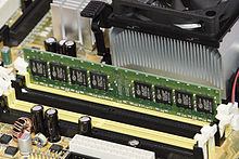
Because of the demands made by increasingly powerful operating systems and software, system RAM requirements have accelerated dramatically over time.  For instance, at the turn of the millennium a typical computer may have only 128Mb of RAM in total, but in 2007 computers commonly ship with 2Gb of RAM installed, and may include graphics cards with their own additional 512Mb of RAM and more. RAM Changes constantly as the system Operates Providing temporary storage for all data required by the Operating System (OS) and software Directly Accessible viewed as a collection of memory location in which program instructions and data are stored Each memory location is referenced by a unique address assigned to it.  The main memory of the computer is faster than external memory. The contents of each memory location are directly accessed using the address of location. Reading and writing of data is done electronically without any mechanical movement.  Volatile memory (data loss

Reading and Writing Operation of SRAM

Image
The diagram below is illustrate Static Random Access Memory (SRAM)Cell for the explanation. SRAM cell is make up of 2 inverters are cross-connected to form a latch .The latch is connected to 2 bit line by transistor T1 and T2 . T1 and T2 can switch opened or closed under control of word line.When word line is ground level, the transistors are turned off and the latch retrains its state. During the Read Operation ,Word line is activated to close switches T1 and T2 . If the cell is in state 1; the signal on b line is high and the signal on b’ line is low.The opposite is true if the cell is in state 0.Thus, b and b’ are always complements of each other’s. The sense /write circuit at the end of the two bit line monitors their state and sets the corresponding output accordingly. While in Write Operation ,the Sense/Write circuit drives bit lines b and b’, instead of sensing their state.It places the appropriate value on bit line b and its complement on b’ and activate the word

Reading & Writing Operation of DRAM

Image
In Dynamic Random Access Memory CELL , transistor acts as a switch to Close (allowing current to flow) when voltage applied in address line or Open (no current flow) when no voltage applied in address line.Address Line also known as word line .Which use to signal the transistor to close or open. During the Write operation ,a voltage is applied on the bit line and a signal applied to the address line to close the transistor.Then the voltage applied on the bit line will transfer to capacitor and store in the capacitor However the capacitor has tendency to discharge and has to refresh to maintain the bit. While in Reading Operation ,the instruction find the bit store using the address line to read the data or bit. When the address line is selected ,the transistor turns on and the charge stored on the capacitor is fled out onto a bit line and to sense amplifier. Sense amplifiers compare the capacitor voltage to reference value to determine the logic 1 or logic 0.The read out from

how to differentiate HTML with HTML 5

Image